C Plane Sapphire Substrate

Surface Analysis Of The C Plane Sapphire Substrate That Was Reused Download Scientific Diagram

Monocrystal Sapphire C Plane Wafer And Test Directions Download Scientific Diagram

China 2 Inch Epi Ready C Plane Sapphire Substrates Wafers For Growth Of Gan Epitaxial Wafers China Sapphire Epiready Wafer

Fabrication And Characterization Of A Ceo2 Buffer Layer On C Plane And Tilt C Plane Sapphire Substrates Sciencedirect

Specification Of 2 R Plane Sapphire Wafer Download Scientific Diagram
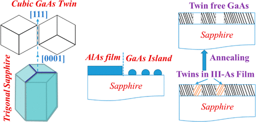
Crystalline Gaas Thin Film Growth On A C Plane Sapphire Substrate Crystal Growth Design X Mol

In order to grow a uniform epitaxial layer of gan across the entire surface the surface of the sapphire substrate is tilted slightly along the c plane.
C plane sapphire substrate.

Sapphire Wafer 3inch C Plane Ostech Co Ltd
Sapphire
Schematic Diagram Of The Surface Atomic Structure Of A C Plane 0001 Download Scientific Diagram

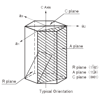
A Coordinate Systems In The Sapphire Crystal And The R Plane And B Download Scientific Diagram

A Tem Bright Field Image Of W Bn Thin Film On C Plane Sapphire Download Scientific Diagram


China Sapphire Substrate Sapphire Plate Sapphire Glass China Sapphire Substrates Wafer Epiready Wafer

Al2o3 Sapphire Wafer C Plane 0001 2 Dia X 0 5mm 2sp Alc50d05c2

X Ray Pole Figures Of A Sapphire C Plane Substrate B Zno Bottom Download Scientific Diagram
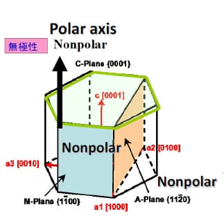
Sapphire Wafer A Plane R Plane M Plane Semi Polar Non Polar Tradekorea

Giwaxs Reciprocal Space Maps Of Mos 2 Films On The C Plane Sapphire Download Scientific Diagram

Analysis Of Cu 111 Crystal Orientation On C Sapphire Substrates A Download Scientific Diagram

A 1 1 µm 2 Afm Topography Image Of A C Plane Sapphire Substrate Download Scientific Diagram

Color Online A Xrd Patterns Of C Cut Sapphire Al 2 O 3 Substrate Download Scientific Diagram

Dsp Ssp M Axis Sapphire Windows Sapphire Wafer 10 10 10 12 2 Inch
Sapphire Single Crystal Semiconductor Laser Diode Using The Same For Substrate And Method For Manufacturing The Same Patent 0792955

Crystal Orientation Of B Ga2o3 Thin Films Formed On C Plane And A Plane Sapphire Substrate Sciencedirect

Pdf Fabrication Of R Plane Sapphire Wafer For Nonpolar A Plane Gan Semantic Scholar

Directing The Morphology Of Chemical Vapor Deposition Grown Mos2 On Sapphire By Crystal Plane Selection Peters 2020 Physica Status Solidi A Wiley Online Library
Source : pinterest.com
